UPDATE (November 24, 2016):
While this blog post still is very popular, it’s a bit old now. It still uses the old Teensy bootloader chip that is meanwhile deprecated and is not available anymore in larger quantities. However, I have been part of the dev team of the new Printrbot Simple 2016 and I have developed the display component which also uses the Teensy. Printrbot made everything open source.
If you are interested in building your own Teensy hardware, have a look in my Behind the scenes report and the Hardware explained report which makes the schematics and PCB available for download. This new PCB features the latest Teensy bootloader chip.
Although the bootloader chip is old that is described here, everything else like routing USB traces is not! Have fun reading it and let me know what you think!
UPDATE (December 15, 2015):
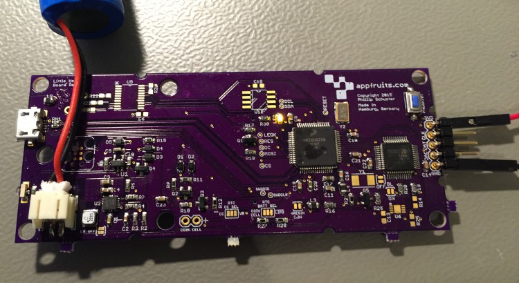
As you are reading this you might be interested in my custom built Teensy project named Little Helper. I made it Open Source under the MIT license including Schematics, Layout, BOM, 3D models of enclosing, and the complete Source Code. Have a look: Appfruits LittleHelper.
UPDATE (June 26, 2015):
Due to popular demand I have created a “reference board layout” and the schematics in EAGLE CAD (7.2) format. I created it by removing all components that were specific to my project. I just left in the Teensy part, the USB-port and a 3.3V regulator and rearranged the components so they fit in a small footprint. I have never produced the board but it should work (also it doesn’t do anything useful) as the components and layout have been working flawlessly in my own application.
This should speed up your development time for your own project. The board layout contains a switching regulator for the 3.3V which might be overkill if you are running your board of an USB-port as the provided regulator is mainly used with LIPO battery based projects and is hard to hand solder (I use a reflow oven which works quite well with QFNs). Use a simple LDO if you are just running your board with USB power. I have left the board layout for the switching regulator as it has been quite hard to get a good board layout with nearly no noise (switching regulators tend to be very noisy due to it’s nature) and should get you up and running quickly if you intent to do a LIPO-based project (of course you will need to add a LIPO charging circuit which can be found for example in Sparkfuns Power Cell product (see board and schematics for details).
All parts have an attribute named MPN for Manufacturer Part Number and MF for manufacturer. This way you can just use EAGLEs BOM-ULP script to export a BOM that you can directly upload to Mouser of DigiKey to get your parts.
Please note: Don’t order the MINI54TAN at DigiKey or Mouser. You will need to order the MINI54TAN at PJRC.com as this IC contains the core Teensy functionality!
You can find the EAGLE board layout and schematics in our Github repository: Custom Teensy 3.1 board layout and schematics. Please make sure to read this blog post before using parts or the whole “reference board” in your own project as there are quite a few things to consider which is largely documented and described below.
If you are reading my blog you might know that I really love Teensy. Teensy is an ARM powered very little Arduino compatible development board. It does one thing so damn good and I think that is very important for a development board and one of the keys to the success of Arduino: Easy programming. You do not need to connect wires and fancy boxes (JTAG programmers), just connect with USB and click on the program button.
But I am not a big fan of using development boards within final products. Although Teensy is really small it’s too high to pack two PCBs together. Using headers for easier soldering and it gets worse. If you really want to build small products you will often have to build your own PCB. Paul Stoffregen, the creator of Teensy enables these efforts by providing the bootloader MCU in his own store. They are very professionell. I had a few issues with german customs and they immediately sent out new ones and I received a refund for the first package that did not make it through.
Of course it’s not Pauls business model to help you out building your own Teensy, although he was very helpful in the forum. You will have to rely on the great Teensy community or blog posts like this one.
As I had a bit of trouble to get my custom Teensy board up and running I will try to give you some advice on how to build your own.
The Teensy schematics
Looking at the schematics gives you a great idea how to build your own custom Teensy. But of course there are a few things left. For example what inductors should be used. And the schematics rely on the USB ports 5V as supply. If you want to use your own supply, for example if you want to use batteries you will have to make a few changes.
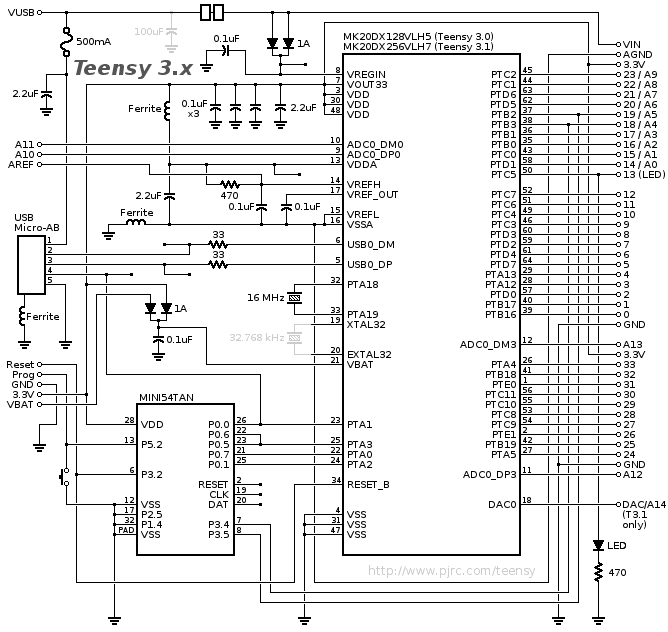
Just to give you an idea how the Teensy actually works: As you can see the boot loader MCU (Mini54Tan) is not directly connected to USB. Only the MK20 is connected to the USB. When you power the Teensy the MK20 will either run the program previously programmed via the Teensy loader (which is triggered by the Arduino IDE) or will wait for the Teensy loader to send a program. Pressing the button on Teensy pulls the P5.2 on Mini54Tan low. That triggers the boot loader MCU which immediately programs the MK20 via SWD (Serial Wire Debug) with a small program that activates the USB part of the MK20 and implements the counterpart of the Teensy loader.
After the MK20s USB is activated it will be discovered by your Mac, Windows or Linux PC. Teensy loader waits for this USB discovery and will then send it’s current program to the MK20.
After I had received my custom Teensy PCBs and soldered the components on it I plugged in the USB cable and it did – well – nothing. I think you know what I am talking about. It’s hard to find an error if you do not know what to search for. I had to know what the MK20 and Mini54Tan are doing so I could find the issue. I had to read a lot of forum posts, ask Paul and others to find out which signals to expect on the different pins.
Signal choreography of the Teensy
When powering up your custom Teensy board you will have a blank MK20, that does basically nothing. If you probe the RESET pin of MK20 you will see a signal like this one:
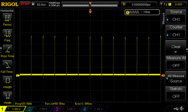
The RESET pin on the MK20 is active low, meaning that the MK20 will be in RESET (programming) mode when the pin is LOW. What you see here is the MK20 being restarted (i.e. RESET goes HIGH) by the watchdog, then crashes immediately with no program found, goes LOW and is restarted by the watchdog 50ms later. I think the correct value is 56ms but my scope showed 50ms in this screenshot.
If you see this signal you know your MK20 is alive and working (so far).
Pressing the Program button, i.e. pulling Pin 5.2 of the Mini54Tan to LOW will also pull the RESET signal of the MK20 to LOW. If you see that, your Mini54Tan MCU seems to be working fine.
When RESET goes LOW after pressing the Program button the Mini54Tan will program the MK20. This is done via the SWD protocol (Serial Wire Debug). That protocol uses a clock and a data signal (like I2C). The clock signal is Pin PTA0, the data signal is PTA3. Probing the PTA0 pin and pressing the program button will show you a typical clock signal on your scope. Then probe for PTA3 (or both at the same time is preferred) and press the program button again. You should now see a typical clock based data signal. If you see that, your Mini54Tan is programming the MK20.

After programming the MK20 the RESET pin will go HIGH, causing the MK20 to run the program (which is the bootloader talking to teensy loader).
In one of my first attempts I got up to this point, but RESET did not go up. I think my MK20 did not receive the program or signal quality of the SWD pins has been corrupted by noise on my power supply lines (likely as I had a lot of noise due to poor PCB layout at my voltage regulator part). If you have a better idea please leave a comment below.
If your own PCB board did make it up to this point you can probe the crystal signal. You should see a nice sinus waveform. Please note: The MK20 will not run the external crystal without a program triggering it. You will only see the crystal signal after the MK20 has been programmed successfully with the boot loader. If you can’t see the signal of the crystal it means that the bootloader program is not running or the crystal could not be brought up due to bad PCB layout or missing connection.

Congratulations: You have a working teensy board. But there is one thing left. Well, to be honest, the most important part is missing: USB to program your board with Teensyduino (Teensys port of the Arduino IDE).
Your computer will now hopefully recognize your custom teensy. USB devices show up with a vendor and a product id. This way the operating system is able to load the necessary drivers. The Teensy will show up with vendor-id 0x16C0 and product-id 0x0483. It’s manufacturer name is „Teensyduino“ and the product name is „USB Serial“. On the Mac and Linux you can run „lsusb“ in a terminal shell to see if such is device is connected and recognized from your computer.
If you can’t see the device you will likely have an issue with the USB part on your PCB board. In one of my earlier devices I brought up my PCB up to this point, the device showed up on my computer, but teensy loader did not manage to program the board as I had poor USB PCB layout causing reflections and poor signal quality.
You can probe the USB+ and USB- pins to see if there is a signal and if the signal is nice and clean. USB is quite robust, but only if you did your part correctely. USB differential pairs need a specified impedance of 90 Ohm. Achieving that on a two layer will require very large track width. The first revision (working up to the USB part) has been a two layer board. In my final board revision I switched to a 4 layer board and used an impedance calculator to get my USB tracks right. I also used EAGLEs meander function to get equal track length of the USB+ and USB- tracks.
Your custom Teensy schematics
Paul offers the schematics of his Teensy as you could see at the beginning of this post. This schematic does a great job, but if you don’t want to use the voltage regulator built into the MK20 you might have some questions how to connect the pins in that case. It is necessary to follow Pauls schematics, meaning that pins like VREGIN, VBAT and VOUT will have to be connected. Don’t let them floating!
Follow these rules if you provide your own 3.3V. I did that as I wanted to run my device from LIPO batteries from my own voltage regulator:
- Connect VOUT to 3.3V and add a 0.1uF capacitor near the pin
- Connect VREGIN to 3.3V and add a 0.1uF capacitor near the pin
- Connect VBAT to either 3.3V or a coin cell battery. Just make sure to provide power.
PCB Layout considerations
There are three different package versions of the Mini54Tan: a TQFP and two QFN packages. Soldering a TQFP package by hand is easier than a QFN package. As I had enough place on my board I chose the TQFP package. Using another package would propably require another layout as the pin positions are different between the packages. You can buy the Mini54Tan MCU in the PJRC Store.
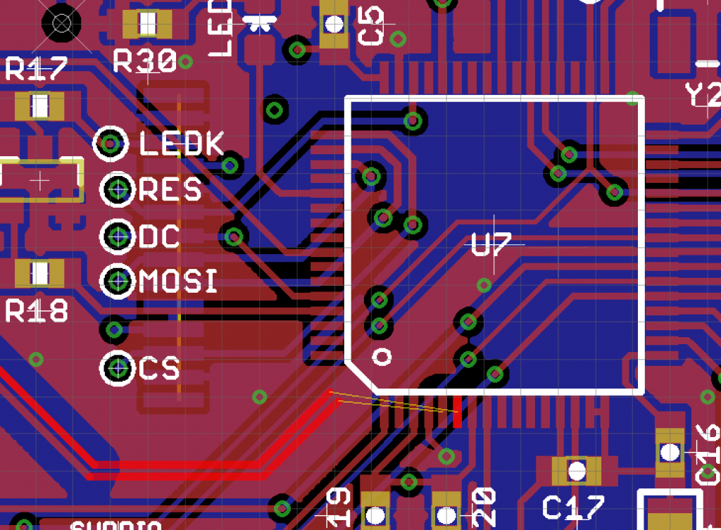
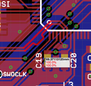
This is a screenshot from my PCB Layout featuring the Teensy part. As said before I am using a 4 layer PCB layout with a rather standard 4-layer stackup with these layers: Top, GND, Power (in my case 3.3V) and Bottom layer. I let my boards get manufactured at OSHPark.
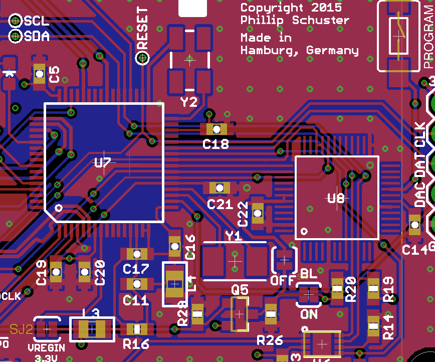
As you can see I placed capacitors (typically 0.1uF) at each power pin of both ICs (C5, C18, C21, C22, C14, C17, C19, C20). I chose ferrite beds (L3, L4) in 0805 packages, the next time I would rather choose 0603 packages as they are a bit smaller. Paul posted the values in one of his forum threads: 600 Ohm/100 Mhz. If you are interested: I have chosen this part: BK2125HM601-T.
By aligning both MCUs as I did you can minimize track length and routing is quite easy between both. If you found a better way of aligning and routing the MCUs please let us know by posting your layout as a comment.
As this is prototype version I added a few jumpers that let me reroute or deactivate features without cutting traces or soldering small wires to small pins.
Calculating USB differential pairs impedance
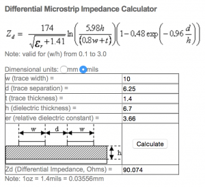
At the bottom left of the MK20 (dot on the left MCU) you can see two tracks coming in from the bottom left of the image. That is the USB signal with the bottom tracks meander that will give both traces equal length. USB requires careful PCB design and should be routed as a differential pair. USB tracks require a very specific impedance. That is a complex subject and there are numerous resources that will help you understanding it. For the more practically orientated tinkerer: You can use a calculator to calculate the trace width and clearance to get a specific differential pair impedance. You will need the PCB stackup of your PCB manufacturer as you need to know the height of the layers and copper fills.
I used this calculator and entered the values from my favorite manufacturer OSHPark. I entered different values for track width and trace separation until I had an impedance of 90.0 Ohm. I have chosen the values of 10 mil for trace width and 6.25 mil for trace separation (clearance).
Setting up net classes in EAGLE
Using these values you can now route your USB traces. I am using EAGLE. In EAGLE differential pair routing is quite simple, but a bit hidden in the software. The first step is to create and set net classes. In EAGLE go to Edit->Net classes. There you can create different values for trace width and clearance. Differential pairs should have quite a big clearance to copper pours (2-3 times the track width). Therefore I entered two net classes, one for USB (#1) and one for the top copper pour (#2) as my USB signal is routed on the top layer. As you can see I entered the values from the impedance calculator in net class #1. 10mil for track width. In Clearance Matrix you tell EAGLE how much clearance the different net classes will be used by the Auto Router or differential pair routing. These settings tell EAGLE that USB traces should be separated by 6.25mil and that USB traces should have a clearance of 30 mil to the traces (copper pours) set to net class #2.
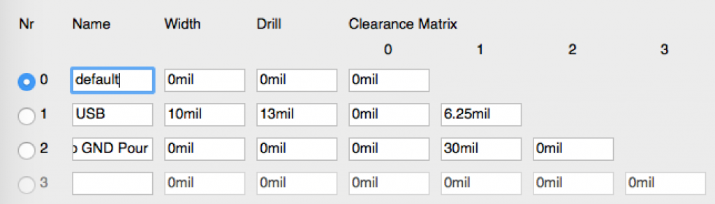
In the next step you have to set the net classes of the traces. I selected each of both USB traces one after the other and set the USB net class in the bottom area of the Info dialog window.
Don’t forget to set the Top GND net class to the polygon forming the top copper pour. If you don’t have a top copper pour you don’t need to do that.
Routing USB traces as a differential pair
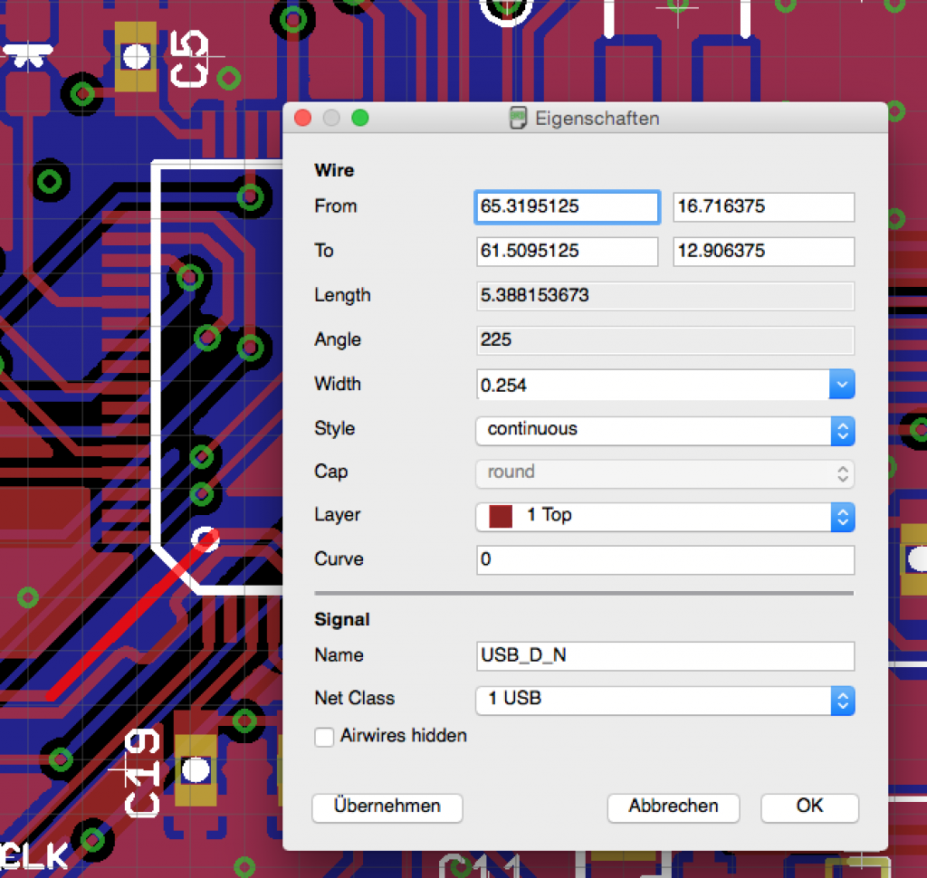
A differential pair is a very interesting method to transfer a signal. A differential pair sends data in two parallel lines. Both lines have the exact same signal at the exact same time, but in opposite polarity. This is why differential pairs are often named with + or – M or P in their signal names. As you can see in the Teensy schematics the USB pins are named USB0_DM and USB0-DP. The signal on one line is HIGH, then the signal on the other line is LOW and the other way round. This way EMI and other radio frequency issues can be controlled resulting in very, very good signal quality and high speed signal transferring. To make that work, both lines have to be of a very specific impedance as said before and they must be routed in parallel with very high precision. If possible (make it possible!) do not use vias, i.e. route the signal on one layer and make sure the signals are in parallel. You should make sure that both tracks have the same length. Routing a differential pair without the right tool is pain in the ass as you have to get the clearance (width of gap between both traces) right all the time. EAGLE can help you with that.
In order to trigger EAGLEs automatic differential pair routing you have to name the signals for USB one ending with _P and the other one ending with _N. I named my signals (using the NAME command in the Schematic Editor of EAGLE) to USB_D_N and USB_D_P. Start the ROUTE command in EAGLE and click on one of the USB traces. EAGLE will now route both traces as one. Press the ESC-key to just route one of them. This is necessary to connect the USB signals to the MCUs pins.
Getting the trace length right
You want both USB traces having the same length (< 1mm difference) To get equal track length you will have to use the MEANDER feature of EAGLE. Activate the MEANDER feature in EAGLE. Press and hold CMD-Button (Mac, consult EAGLE manual for Windows keys) and click on the first USB trace. EAGLE will show a small tool tip showing the length of the track. Now – while still holding down the CMD key – click the other track. EAGLE will show the next value with the track length. Now click one of the tracks and move your mouse – sometimes you have to really move far away in order to see an effect. EAGLE will try to route both traces to equal length. Press the right mouse button to switch between both traces and the shorter trace. I routed the shorter trace with a small loop. Sometimes EAGLE will just do nothing, move your mouse around the screen until you see an effect. Then precisely move your mouse to position the meander as you like. It will take some time to get used to this feature. Just play around with it. There are a few screencasts on YouTube that show you exactly how to meander traces in EAGLE.
I am just scratching the surface of differential pair routing and high speed PCB designs. This is a very complex, yet interesting part. Google is your friend. Trade has very good general infos on high speed design guidelines with a very good part on differential pair routing. The document can be found here.
Some tips and tricks for your own custom Teensy
I needed two revisions to get my custom Teeny board working. There were numerous issues I had from starting my project to the first blinking LED on my own board. Here are a view guidelines you should follow:
Add test points
In my first boards revision I did not add any test points. My board did not work and I had to position the needle of my probe to very, very short pins. Holding them there while trying to press the program button was not easy. That was a very frustrating way of checking a board. I had to try a few routes (i.e. connecting VOUT to 3.3V) and had to solder small wires to very small pins. That was not an easy task. If I had test points that would have been very easy to do. If you have the space, implement some test points for the most important signals.
Add jumpers
Perhaps you will have to reroute some traces. Perhaps you have implemented features that you did not fully prototype. Cutting traces is one way, the better way is to use jumpers. You can see a few of these jumpers in my PCB layout. As everything worked out fine so far I did not have to use them, but it made me confident to get my board working even if I did something wrong in my PCB layout or schematics.
Add LEDs
I also add one or more LEDs to my custom PCBs. My current project will be fully enclosed. And I don’t plan to use them in production code, I might even let them out (not soldering them on the board). But they are very, very helpful in your own custom PCBs. It’s awesome to see a LED blinking after hours playing with your board and fighting to get it up and running. And they are very helpful to quickly show if everything is working fine.
Use one LED and connect it to a free pin of your MCU (typically there is one floating pin left in every design). I have read somewhere even the latest Nexus smartphone as a LED that is not used ;-).
Double check and then triple check again
In my first revision of my PCB I had some issues that I hardly could prevented as I just did not know – one reason why I have written this blog post so that you know! But I also had some issues that were just introduced because I did not triple check it. One GND pin of my voltage regulator simply had no connection. You should reset your DRC before sending your design to production and accept errors one by one again. Sometimes DRC errors that were ok while developing your PCB but in your final design they will be an issue. So clear DRC errors and run the test again. Make sure you loaded the DRU from your manufacturer before to check the correct parameters.
That’s it. I really hope that this blog post can help you with your own custom Teensy. Paul did a tremendous job with the Teensy and I think your own custom PCB will benefit from it’s work by being easily programed. And don’t forget: You get full Arduino compatibility but with high speed. Programming powerful ARM has never been so easy.
Consider your soldering skills to be an issue
As said numerous times before I had a hard time getting my board up. Hardware is hard. Because you do not really know what’s wrong with a completely new board. There are so many possible failures. But, you have prototyped your schematics, you have double and triple checked your PCB layout, you trust your manufacturer. But, there is something you never should trust: Your own soldering skills. If a lot of reasons exist for something to fail it’s often the easiest one. And in my case it’s soldering skills. My board did not work because the voltage regulator (being a QFN package with nearly invisible pins from the outside) did not reflow correctly with my Hot Air Soldering Station. I removed the device and soldered it again on my board and voila – everything worked out nicely.
Take care of your USB part
It’s kind of annoying having a working board but communication fails due to bad USB design. A big part of my blog post is dedicated to this part. USB traces should be routed as one of the first tracks to get them as straight as possible. If you have corners follow principle design guidelines.
There is a very good document created by Toradex describing high speed design guidelines. They have a very good part on impedance, differential pairs and generell PCB layout design considerations. You can find the document here.
Setting your own USB manufacturer and vendor IDs
As said before Teensy is recognized by its USB vendor and product ID. Perhaps, i.e. for a commercial product you might want to set your own. I will not get into details as this can be done later in software, you don’t have to care about it when designing your PCB. There are numerous forum posts regarding this subject. You might start here: How to change the Teensy product name.
Of course I am very interested in your ideas. Please let me know if something is wrong or could be better done or explained. If this blog post helped you designing your own product please leave a comment below.
Careful crystal design
It’s very important to take care of your crystal design. The 16 MHz crystal is Y2 in my PCB layout (see above). You can see that I place the crystal as near as possible to the MK20. Also make sure no other traces are below the crystal (if you are using a 2-layer PCB, in a 4-layer PCB you can route a trace at the bottom layer as the GND and Power are in between). Just follow my layout and you will be fine. Paul did write down a few other considerations regarding crystal layout, so give it a try.
To make your own life easier: I have chosen this part and it has been working great: ECS-160-8-30B-CKM.
One last thing…
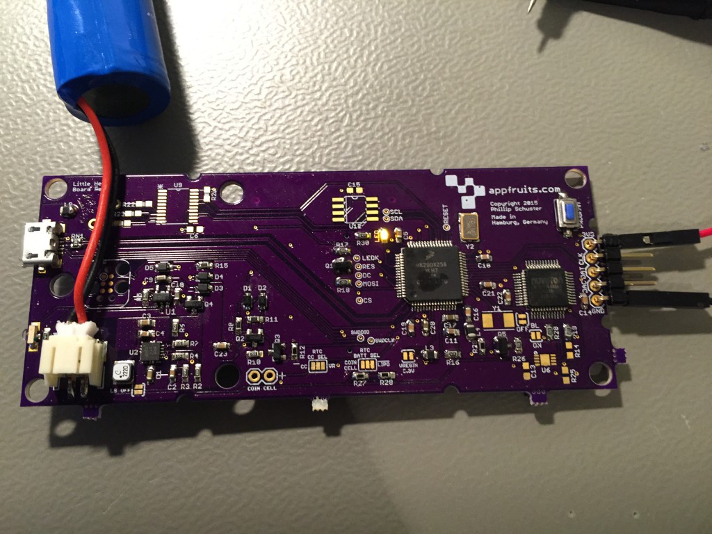
Perhaps you want to know what I did create with my custom Teensy project. Well, it’s called Little Helper. It’s an electronics tinkerers best friend. A few days ago I managed to get the main board up and running, but there are various components left that must be soldered on the PCB and a few other components must be connected to it (on the backside) so get a fully working device. But here is an image of the main board with blinking LED…
I’ll let you know what it is supposed to do as soon as I have a completely working device. I hope to get that done in the next few weeks. But you know: Hardware is hard. It could take a bit longer ;-).
Good luck.
Phillip


Hi Phillip!
Thanks for this post, it’s really helpful and I have to confess I’m mostly ripping it off in order to design my own custom teensy based pcb.
Still just at the beginning of the design placing components in the schematic in Cadence whenever I got some time to spare at my workplace. The thing is that I want to use a type-B USB connector instead of the micro-AB in my design. I’ve noticed that the pin-out slightly differs between those and that the 4th pin labeled “ID” that the micro-ab has, doesn’t exist in the type-B. Also I can tell from Paul’s schematics that it is attached to the mini54 and to the mk20, maybe to tell when each of those it’s suposed to work? Do you think that overriding it can cause problems when uploading sketches or something?
Thanks a lot in advance and keep up with the great job on this blog!
Oscar.
Hi Oscar,
thank you very much for your feedback. I really appreciate it. The ID signal is used for USB On-The-Go (OTG). More Info here: http://en.wikipedia.org/wiki/USB_On-The-Go. To summarize it: A smartphone is both a USB client and a USB Host. Connecting the smart phone to your PC/Mac will run it as a client, the PC/Mac will transfer data from and to the smartphone (Images, Music, you name it). But, you can also connect a digital camera to your smartphone. Now the smartphone is a hub, taking command of the connected device. To make that possible the ID signal has been added to the USB specification.
As far as I know ID line should be HIGH if you are running in client mode and LOW if your device runs in OTG mode. I fired up my scope and measured the ID signal (test points really rock ;-)). I booted my device, ID goes HIGH, I pressed Programm button and uploaded a new sketch, ID stays HIGH, I stopped my device and ID (naturally) goes LOW.
Here is a screenshot of my scope showing the ID signal: http://www.appfruits.com/?attachment_id=241
I think you should be fine by letting the USB ID signal floating or pulling it high. If you have the board space I would add a 3-way solder-blob jumper providing HIGH, LOW and floating (not connected to anything). This way you can find the right settings for your board.
Paul has a lot of experience with USB. I would ask in the Teensy forum. Please come back to me if you know for sure so I can update my article.
Phillip
Phillip, is there any chance you could make contact, as I’d like to talk to you about you custom Teensy… I’m doing the same thing, but with a difference.
Thanks, Ben
Hi Phillip, this entry is really good, congratulations!
I am facing the design of a custom teensy board too and, I am having some troubles that are quite similar to the ones you explain, however I can’t solve them!
The thing is that once I mounted the received PCB prototype, the board was working, but after some days is not… The board is able to load the bootloader part, I can see it as an HID device implementing the hafkey protocol, in theory there is a succesful communication between the teensy loader and the board since the programming sequence looks like normal BUT, once it reboots, no program is running on it, it looks like ‘dead’ (there is no clock signal after the program has been transfered).
Summing up, right now, every time I press the program button, I can see the HID address and program it, but after this, nothing happens. Did you have something similar during your design?
If you have some time I would like to comment some changes I did on the supply part that, at least, for several times they were working and can help you to improve consumption for your battery based application.
Thanks in advance,
Nacho.
I had very similar problems with my first prototype. I had a long discussion in the PJRC.com forum. It turned out my power supply killed the MK20. But that was a very specific problem and I don’t think it’s exactely the same problem in your case. But it might help that voltage peaks kill the MK20.
You can find more info here: https://forum.pjrc.com/threads/27703-Custom-build-Teensy-3-1-PCB-not-responding
You will find a lot of screenshots of my oscilloscope that should help to visualize the problem.
Hope that helps a bit.
Phillip
Hi Phillip,
Thank you for the nice information about Teensy! It is very helpful.
While I was comparing your schematic to the one from PJRC, it seems that yours doesn’t have I2C (P3.4, P3.5) connection to MINI54. I tried it and it worked very well. However, I wanted to change the TQFP to QFN5x5 and then I was wondering if there won’t be any difference or problem. I wired them up as the PJRC MINI54 connection table suggested.
Another issue could be that if we wire 2 Teensy modules with the MINI54 chips together, then it seems that I2C can have an issue since the address must be different.
I wanted to ask you how you would think of these issues.
I will look forward to hearing from you!
Thank you,
Sung
I had a discussion regarding the I2C part and it turns out it is never used. Paul said in the discussion:
https://forum.pjrc.com/threads/27703-Custom-build-Teensy-3-1-PCB-not-responding?p=76564&viewfull=1#post76564
Hope that helps,
Phillip
Hi Phillip..
Thanks for this Really Helpful Information..
Hey, I used your schematic in a design and the regulator is giving out 3.9v. I was able to detect the teensy though and program it. However, now it seems like the board is broken because I cant program it anymore.
Do you have any idea about how to fix this power supply issue? Also do you think that the MK20 is fried now?
So sorry about my late answer. This comment got caught by my damn Spam filter. Do you have an oscilloscope? Do you use the exact same regulator part?
Phillip,
Great site! I’ve used your instructions as a starting point, but I’ve rearranged things and eliminated the Y2 crystal. Teensyduino tells me that my upload is successful, but I can’t get the board to do anything and the serial monitor can’t find the board. Any suggestions where I should look?
-Brett
Nevermind! I’m not sure what I did but it’s working now. I think reflowing the crystal did it (Y2 not Y1) but I’m not sure.
Hey Phillip awesome article. We recently started a kickstarter using the Teensy 3.2 and it has taken off so much that I think we are going to have to build a custom Teensy. Would you or anybody else be interested in helping us out it is a pretty interesting project https://crp.to/ok one thing we are looking for though is someone with the ability and experience to build the custom teensy. Feel free to contact me for more info.
Tim
Excellent tutorial !!! Super detailled, really it’s perfect 🙂
Now only thing is to update the schematic with the MLK02 ^^
Could we have a rough idea of the cost (parts) to build a custom teensy in regards of a stock Teensy 3.2 ?
Thanks a lot 🙂
I have already ordered the new bootloader chips from PJRC and created an updated PCB based on the Teensy 3.2 design. I will update this post as soon as I have verified that the updated layout is working fine. Regarding costs: You’ll have to buy the bootloader chip from PJRC which is rather expensive with about $6. The MK20DX256LH7 (the main MCU) is about $5-$6. You’ll need a few chicken foot components (caps, resistors) which add around $0,5-$1. You’ll also need a USB connector and a programming button, which add another $1 – $3 depending on which models you choose. All in all it’s not cheaper to create your own clone as you have to add PCB manufacture costs, shipping fees. If course you can drop the costs if you create hundred or thousands of them. But the Teensy bootloader kills any “clones” – which is by design I think ;-).
I’m having trouble bringing up a custom Teensy based on a MK20DX128VLH7. I’m compiling the “Blinky” code as a Teensy 3.0. I have verified that the reset line, data/clock, and USB lines are valid and have good signal quality.
My problem is if i build and upload, the build works, the Teensy loader starts but, after a timeout, I get the message to press the Program Mode button since the board didn’t respond to a USB-based reboot request. If I scope the reset line and press the program button the normal pulses which are about 56us apart go to a solid up level and my PC gives an error message: the “USB Device not recognized”.
At this point, probing the crystal shows the MK20 oscillator is running. I have also verified clean 3.3V on the 3 MK20 VDD pins plus 3.3V on VBAT and VREGOUT. There are multiple 100nF decoupling caps in place on the 3.3V pins. The board has a ground plane and there are no traces under the crystal. USB DM and DP are of the correct polarity at the MK20 pins. I have also tried using the Teensy Loader to open the hex file and load it.
My setup is OK as it works fine with a Teensy 3.2 (with the IDE set for the different board).
So I would welcom any ideas on what else to check or could be wrong. I am out of ideas at this point!
Hi,
that all sounds not too bad. Having a reset signal with these 56us spikes shows that your MK20 is working fine (but doesn’t have a firmware) and pressing the program button pulling reset low and then high means that the bootloader chip uploads the USB bootloader firmware to the MK20 which takes the connection to the PC to get the firmware. All that sounds good. But there seems to be an issue with USB. Do you use a 4 layer board with traces on top and bottom and GND and 3V3 as the inner layers? Did you take attention to the impedance of the USB traces? I.e. did you check out the layer stackup of your board house and adjusted the USB traces width and distance? May I ask where you have manufactured your board? Did you add a 30 ohm resistor close to the USB port on the DP and DM USB signals which is called a terminating resistor and which adds to signal quality by removing reflections.
I hope I can help.
Phillip
Thanks for the quick reply, Philip. Yes… to all of your questions.
I posted a similar question on the Teensy forum and Paul has responded that my problem is that I am using the MKL04 bootloader chip which doesn’t support a 128K MK20. Only the Mini54 does. I picked the 128K over the 256K strictly for cost but do have some 256L MK20s so will try mounting one of those to see if it it fixes my problem.
Thanks
Al
What is your stack-up for the 4 layer board ?
This design is optimized for the OSHPark 4-Layer stackup: http://docs.oshpark.com/services/four-layer/.
Hi Phillip,
just a little question: as i’ve read on the k20 datasheet the VREG_IN pin, if unused, should be connected to GND with 10k. You suggest to connect to 3.3V with 0.1uF.
What should i do and why?
Thanks a lot!
Hi Phillip!
I have a question in design a diy teensy. Teensy mainly based on MK20DX256VLH7. And the pre-loaded bootloader chip make it possible for teesny to load arduino code.So if a want to design a teensy based boad.I can just make two board. One is pre-loaded bootloader board with a small bootloader chip and Micro usb on it. The other have MK20DX256VLH7 and the left.Is that right? Do you have any experience if the bootloader chip must be attached to the main board anytime?It is impoartant for me,because I want to design a very small board. And I want about 1000 main board,so I think it’s worth making a new design. Any suggestion?
Thank you,
Andy
Hi Phillip,
I have a question in design a diy teensy. Teensy mainly based on MK20DX256VLH7. And the pre-loaded bootloader chip make it possible for teesny to load arduino code.So if a want to design a teensy based boad.I can just make two board. One is pre-loaded bootloader board with a small bootloader chip and Micro usb on it. The other have MK20DX256VLH7 and the left.Is that right? Do you have any experience if the bootloader chip must be attached to the main board anytime?You know it is impoartant for me,because I want to design a very small board. And I want more than 1000 main board,so I think it’s worth making a new design. Any suggestion?
Thank you.
Andy
Hello,
why does it need a MINI54TAN to be programmed ?
cant I just use a random SPI/SWD programmer ?
what’s the story about this?
regards
“why does it need a MINI54TAN to be programmed ?”
It’s a feature of the PJRC Teensy platform which enables compatibility with the Teensy loader. The benefit is compatibility with the Teensy software eco-system (teensyduino), and a virtually unbrickable platform. There’s no bootloader stored on the main MCU to overwrite, the firmware loading is handled by the pre-programmed bootloader chip. So no matter what you program to the Teensy there’s always a way to send a new firmware. The exception is if you send firmware that sets fuses.
The MINI54TAN has been replace by the MKL02.